Features
1. Design Flexibility
Multi-layer boards offer great design flexibility. They can achieve more complex circuit routing through interconnections between layers and provide additional layers for organizing and arranging circuit components. Moreover, multi-layer boards can be stacked or separated as needed to meet various functional and performance requirements. This versatility makes multi-layer boards widely used in advanced electronic products and telecommunication equipment.
2. High Integration Degree
Multi-layer boards can integrate multiple functional layers within a single circuit board, achieving a higher degree of integration. By placing different signal layers, power planes, and ground planes between layers, the routing length can be effectively reduced, thereby improving the operating speed and performance of the circuit.
In particular, HDI multilayer PCBs feature smaller board sizes, making electronic products more compact and lightweight. In addition, HDI multilayer PCBs include blind and buried vias, which enable more flexible interlayer connections.
3. Anti-Interference Performance
Multilayer circuit boards enhance the circuit's anti-interference capability by incorporating shielding and ground layers between signal layers. Shielding layers help isolate signal interference between different layers, preventing signal crosstalk and electromagnetic radiation, thereby ensuring circuit stability. Ground layers provide an excellent grounding plane, reducing the signal return path and voltage noise.
4. Signal Reliability
A distinctive feature of multi-layer boards is their signal reliability. By allowing vertical signal transmission between layers, they can shorten the transmission path and reduce coupling effects, improving the stability and reliability of signal transmission. Additionally, multi-layer boards offer better impedance matching performance, meeting the requirements of high-frequency circuits and signal transmission.
Conclusion
Multilayer circuit boards offer several key advantages, including higher integration, better signal integrity, greater reliability, and improved anti-interference performance. These features make multilayer circuit boards ideal for use in complex circuit designs and high-performance electronic systems.
Consturction
Structural Composition of Multi-Layer Circuit Boards
The structural composition of multi-layer circuit boards mainly includes conductive layers and dielectric layers.
Multilayer circuit boards are typically formed by alternately stacking multiple conductive and dielectric layers, with each pair of conductive layers separated by a dielectric layer. The conductive layers are used for circuit routing, while the dielectric layers provide insulation and mechanical support.
Multilayer circuit boards can be classified into different types based on their structure, including common through-hole boards and HDI boards.
Through-Hole Board:
The most common type, formed by drilling holes and applying copper plating to create interlayer connections. It is suitable for circuit boards with various numbers of layers.
HDI Board:
The High-Density Interconnect board features holes on both surface and inner layers, created using laser drilling technology. It is ideal for high-density wiring applications that require compact size and high performance.
Application
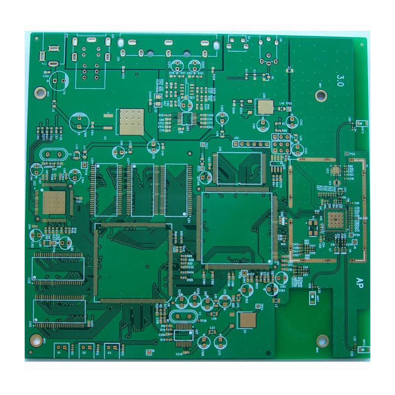
Multilayer circuits boards are widely used in various electronic product, such as smartphones and computer motherboards. Circuit boards with different numbers of layers are suitable for electronic devices of different complexities.
Common Specification
FR-4, 1.6mm board thickness, 1oz copper, finish: HASL,,ENIG ,Gold plating ,etc.
Common types:
HDI multilayer boards can be categorized into three common types based on their process and structure:
First-Order HDI (Basic Type)
Consists of a core layer with blind-via layers on both sides, suitable for mid-range smartphones, consumer electronics, and similar products.
Second-Order HDI (Advanced Type)
Adds an additional blind-via layer on top of the basic type, supporting higher interconnect density, suitable for flagship smartphones, tablets, and other complex devices.
Any-Order HDI (High-End Type)
Achieves extreme density through interconnections between any two layers, commonly used in high-end chip modules (such as Apple A-series packages) and serves as a precursor structure for System-in-Package (SiP) designs.
Customized product:
Most of our products are customized based on the original Gerber files provided by our customers.
After receiving the original Gerber files, we convert them into working Gerber files for production use.
During this conversion process, we adjust certain parameters-such as hole diameter, trace width, and trace spacing-to optimize manufacturability and ensure smooth production.
Package and warranty:
All our products are vacuum-packaged with desiccant to ensure optimal protection during storage and transportation.
The shelf life of vacuum-packaged circuit boards varies depending on the surface treatment process, typically ranging from 3 to 12 months. The details are as follows:
Shelf Life for Different Surface Treatment Processes
ENIG (Electroless Nickel Immersion Gold):
Can be stored for up to 12 months under vacuum packaging with desiccant protection.
Lead-Free HASL (Hot Air Solder Leveling):
When no special storage adjustments are made, the shelf life is typically about 3 months.
OSP (Organic Solderability Preservative):
Has a shelf life of 3–6 months under vacuum packaging with desiccant protection. However, if stored improperly (e.g., without desiccant or with insufficient vacuum sealing), the shelf life may shorten to around 3 months.
Immersion Gold (Chemical Gold Plating):
Shelf life can reach 6–12 months, provided that sealed packaging and desiccant are used.
Company advantage :
1, We guarantee a response within 24 hours to all customer inquiries and complaints.
2, Our factory offers 1-day sample production for 2-layer boards and provides rapid manufacturing services for small and medium orders, ensuring short lead times and on-time delivery.
3, We support multiple payment options, including EUR, USD, RUB, and CNY, through PayPal, T/T, and other convenient methods.
Hot Tags: hdi multilayer pcb, China hdi multilayer pcb manufacturers, suppliers